Investigation of residual stresses in bulk single crystals for piezoelectric sensors using Neutron Diffraction
Kistler is the world market leader in dynamic measurement technology for recording pressure, force, torque and acceleration. As an experienced development partner with unique sensor technology, Kistler enables its customers to optimize their products and processes and create sustainable competitive advantages. Around 2,000 employees at more than 60 locations worldwide develop new solutions every day and provide application-specific services on site.
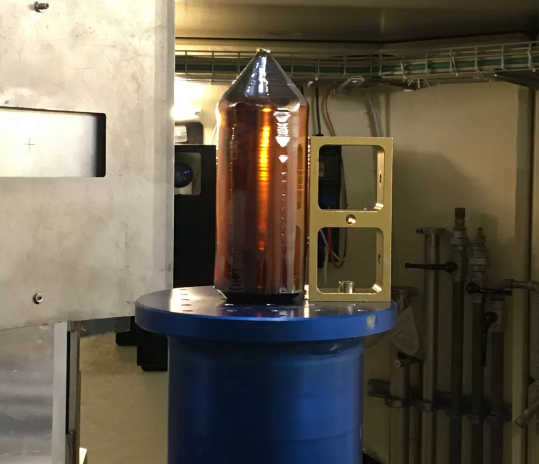
At Kistler, the heart of the sensors is made from piezoelectric single crystals grown at the headquarters in Winterthur (CH) using the Czochralski process at temperatures of up to 1400 °C. The crystals are grown in a single step. The growth of a Ø 55 x 150 mm crystal (weighing 1.5 to 3 kg) usually takes eight to ten days. The cooling phase in particular represents a major challenge: It has to ensure that as little residual stress as possible is generated so that the crystal does not crack during cooling or at a later stage during further processing. Kistler's aim is to install only high-quality crystal elements in its sensors so that the sensors, which are used at high temperatures and under high loads, function perfectly. It is therefore central that crystal elements that are as stress-free as possible are used for the end product. Determining the residual stresses in a crystal is not an easy task, especially if the crystal is only partially transparent to light. In its search for a suitable method, Kistler asked ANAXAM for its expertise in measuring residual stresses.
The applied material analytics of ANAXAM using Neutron Diffraction helps Kistler to better understand the internal stresses that occur during the growth and cooling of its crystals. The analysis is ideally performed on "as-grown" crystals so that the image of residual stresses corresponds to the effective state of the crystal after cooling. 3D mapping allows zones with higher residual stresses to be not only qualitatively identified, but also quantitatively evaluated. The determination of process parameters, can now be performed more efficiently, based on reliable data.
Kistler can transfer the results achieved by ANAXAM directly to the optimization of its internal process and thus reduce scrap in the production of crystals in the future. The higher crystal quality is also reflected in the yield in further processing steps, such as wafer separation or grinding of small components. Ultimately, the quality of the crystal elements produced increases - a win-win situation for Kistler and its customers.
For this customer project, ANAXAM used POLDI beamline at the Paul Scherrer Institute.
Thanks to ANAXAM's expertise, we were able to create a 3D mapping of the residual stresses in our crystals for the first time, which allows us to optimize the growth process on a scientific basis.”
Dr. Roland Sommer, Head of the Piezoelectric Technology Group, Kistler Instrumente AG
The measurements were carried out efficiently and within the available beamtime. The Kistler team was able to be up close to the preparations and the measurement process on site and thus also gained an exciting insight into the world of neutron scattering.”
Dr. Pirouz Sohi, Piezoelectric Sensor Technology, Kistler Instrumente AG